Cleanroom Classification for Key Processes
Table 1: Cleanroom Class Requirements for Major Electronics and Semiconductor Manufacturing Processes
| Process Step |
Cleanroom Class |
Particle Size Controlled |
| Wafer manufacturing |
Photolithography |
ISO Class 3–4 |
≥ 0.1 μm |
| Thin film deposition, etching |
ISO Class 4–5 |
| Packaging & testing |
ISO Class 6–7 |
≥ 0.3 μm |
| Other manufacturing areas |
MEMS |
ISO Class 4–5 |
≥ 0.2 μm |
| Display panels and optoelectronics |
ISO Class 5–7 |
≥ 0.5 μm |
Key Environmental Parameters
Table 2: Key Environmental Parameters for Electronics & Semiconductor Manufacturing Cleanrooms
| Environmental pParameters |
Control Requirements |
Rationale |
| Temperature |
22±1 °C |
- Ensure stable operation of precision equipment (e.g., lithography and alignment systems)
- Minimize thermal expansion impact on lithography and alignment accuracy
- Enhance process consistency
|
| Humidity |
40% – 50% RH (±5%) |
- Prevent electrostatic accumulation
- Avoid moisture condensation
- Maintain the stability of photoresists and chemical performance
|
| Pressure differential |
Clean area maintains positive pressure relative to non-clean area, typically +5 Pa to +20 Pa |
- Prevent infiltration of external contaminated air
- Ensure airflow moves from high-cleanliness areas to low-cleanliness areas
|
| Airflow pattern and velocity |
Vertical unidirectional flow |
0.3–0.45 m/s |
- Unidirectional flow rapidly removes particles in critical processes
- Turbulent flow is cost-effective for general areas
|
| Horizontal unidirectional flow |
0.2–0.45 m/s |
| Turbulent flow |
Controlled by ACH, typically 30–60 AHC |
| Electrostatic control |
106 – 109 Ω |
- Prevent electrostatic damage to wafers, chips, and photoresist
- Ensure operational safety
|
| Noise |
≤ 65 dB |
- Maintain alignment accuracy of lithography and inspection equipment
- Ensure personnel comfort
|
| Vibration |
< 250 μm/s2 |
Primary Contamination Sources
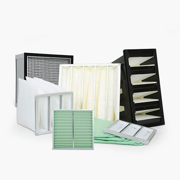
 Product
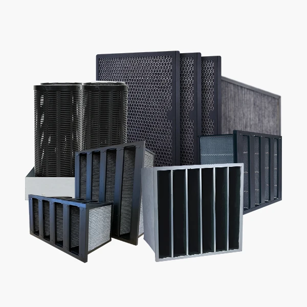